# 英伟芯 / 光电融合带来下一代摩尔定律 - ID: 424 - URL: https://www.stoyard.com/works/424 - English URL: https://www.stoyard.com/en/works/424 - Year: 2025 - Cover: https://static.glabcms.stoyard.com/stoyard/project/cover/20260413/0behk4kxmre.jpg - Categories: 活动、展览设计服务, 中小型企业网站方案, 标志设计, 先进制造, 社交媒体传播、互动H5, 通信、芯片半导体 - English Categories: Event & Exhibition Design, Products Marketing Website, Logotype, Advanced Manufacturing, Social Media/H5 interaction, Semiconductors and Communications - Author: STOYARD - English Author: STOYARD - Publish: 2026-04-01 - Editor: STOYARD BEIJING ## 中文主体 ### 项目简介 英伟芯(西安)科技有限公司成立于 2023 年 12 月,是一家全球化的光电集成技术公司。致力于为数据中心光互连等领域提供高性能的光电集成和硅光解决方案。 其技术方向融合了硅材料的成本效益与光子学的高带宽特性,广泛应用于数据中心、5G 通信、人工智能等多个领域,显著提升了数据传输效率并有效降低了系统能耗。企业主要以异质集成技术为平台基础,开发电芯片(硅基材料)和光芯片(化合物材料)并进行光电融合,瞄准 AI 数据中心光互连、红外探测器等新兴市场。 [Video](https://static.glabcms.stoyard.com/stoyard/gallery/20260414/s9qzdq4fk38.mov) 本标识以公司核心技术——光电集成为设计灵魂。通过极简的几何语言,将“光子”的高速动态与“电子”的稳固基石相融合,体现了英伟芯在硅光芯片领域实现高性能、低能耗数据传输的技术追求。 字母“N”的重构: 图标主体由品牌首字母“N”演化而来,具有极高的辨识度。它不仅代表 NVISION,也寓意着 New(创新)、Next(未来)与 Nano(纳米级精度)。 光电融合的轨迹:左侧实块代表稳固的硅基材料与电路系统(电芯片),象征企业的技术积淀与产业化能力。 圆润弧线:模拟光波的传播路径与光纤形态,展现了光子技术的高带宽与轻盈感。 交汇点:弧线与色块的完美嵌入,精准直观地诠释异质集成这一核心竞争力——即光芯片与电芯片的深度耦合。 动态感与速度: 图标整体呈斜向上的态势,象征着数据在数据中心与 AI 算力网络中的极速传输,也预示着企业在半导体赛道的快速崛起与蓬勃生机。 精密比例: 如辅助线图所示,标识基于严谨的黄金比例与正圆切割而成。这种工程美学的运用,映射了半导体封测环节对“微米级”精度的极致要求,传递出企业对产品品质的工匠精神。 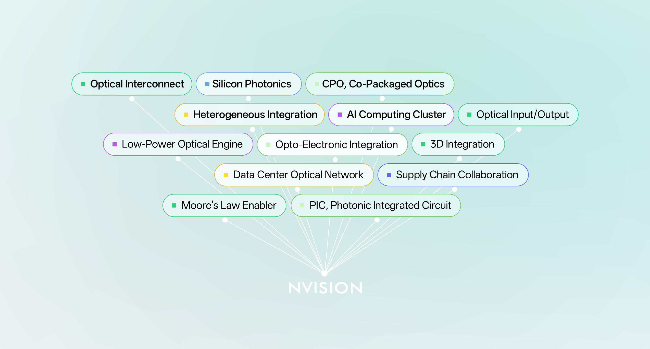 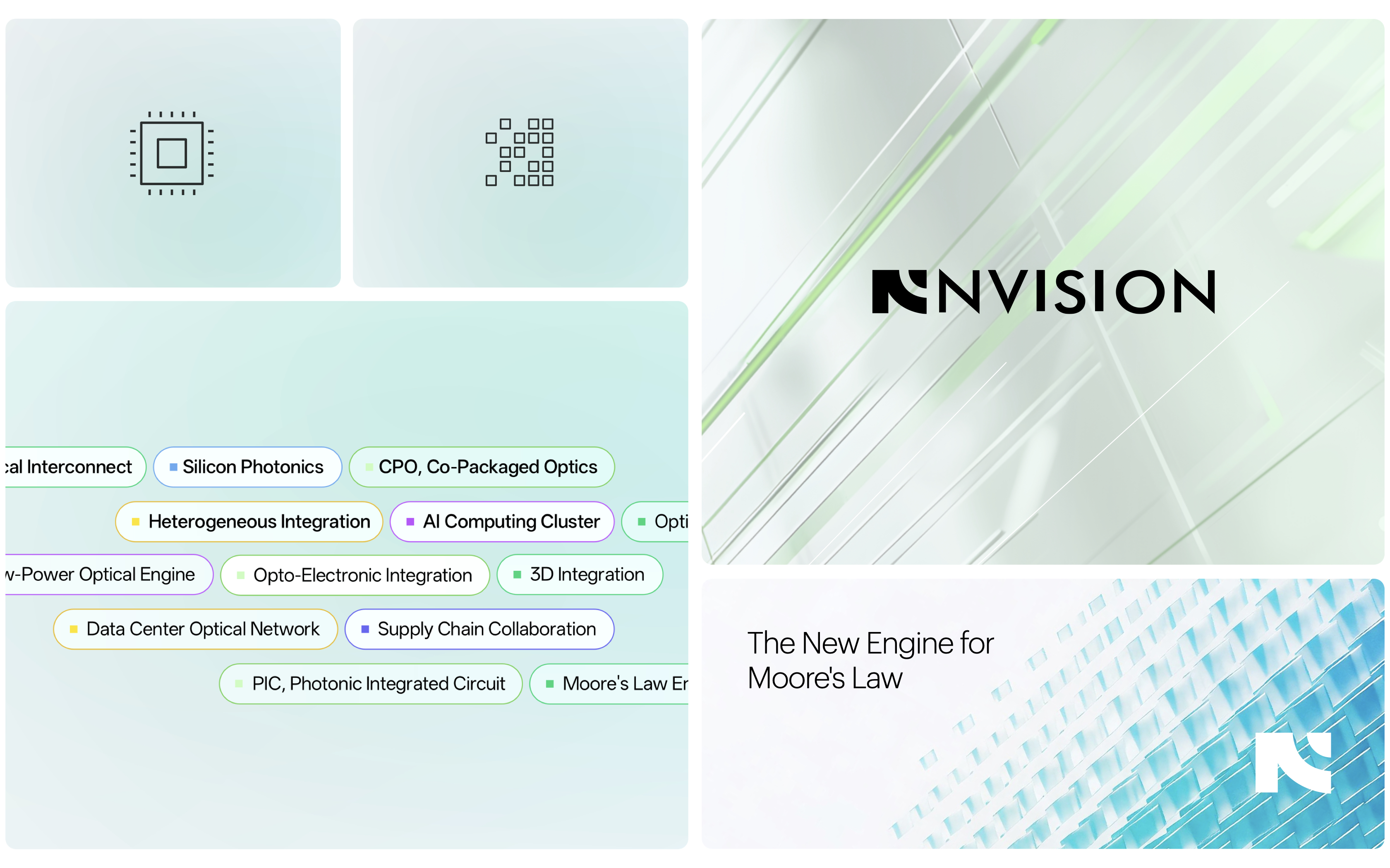  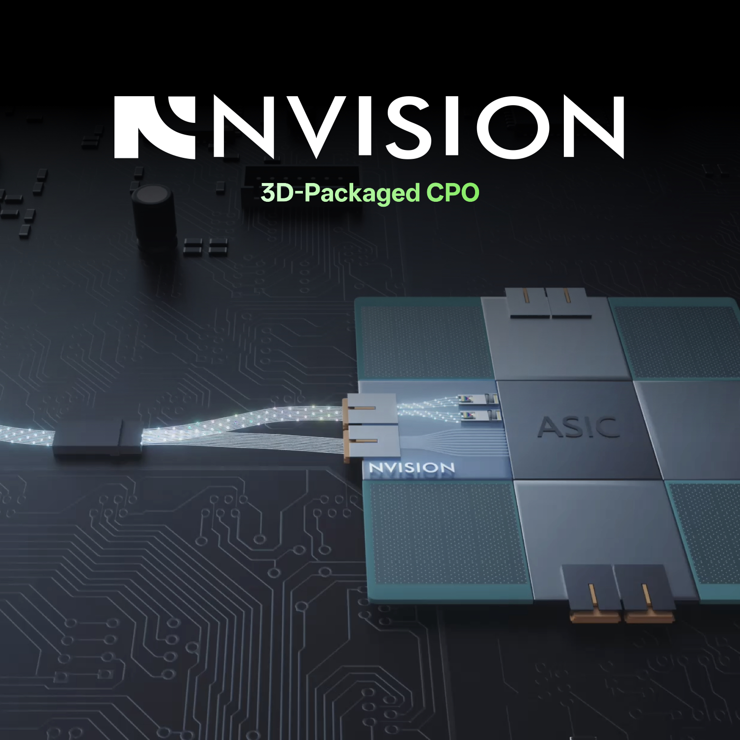 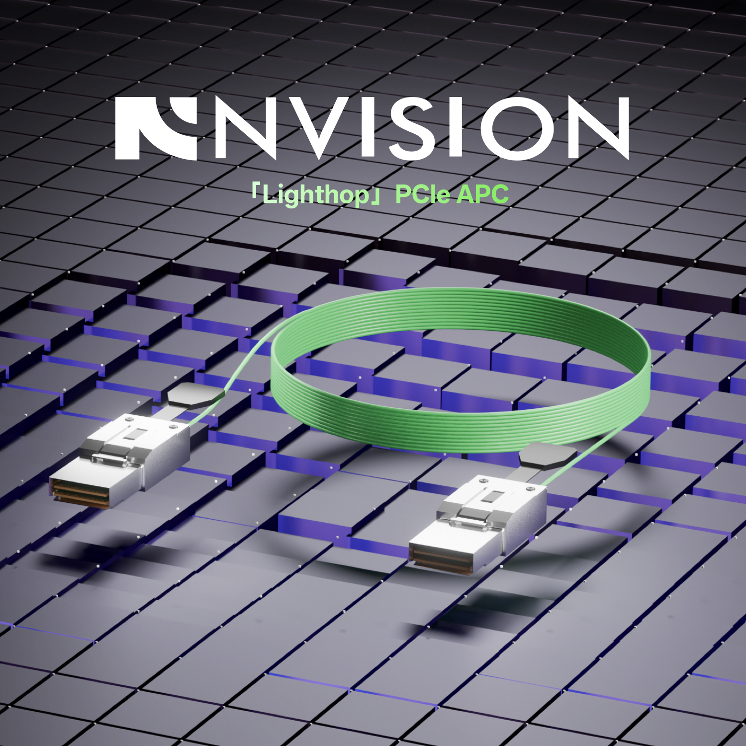 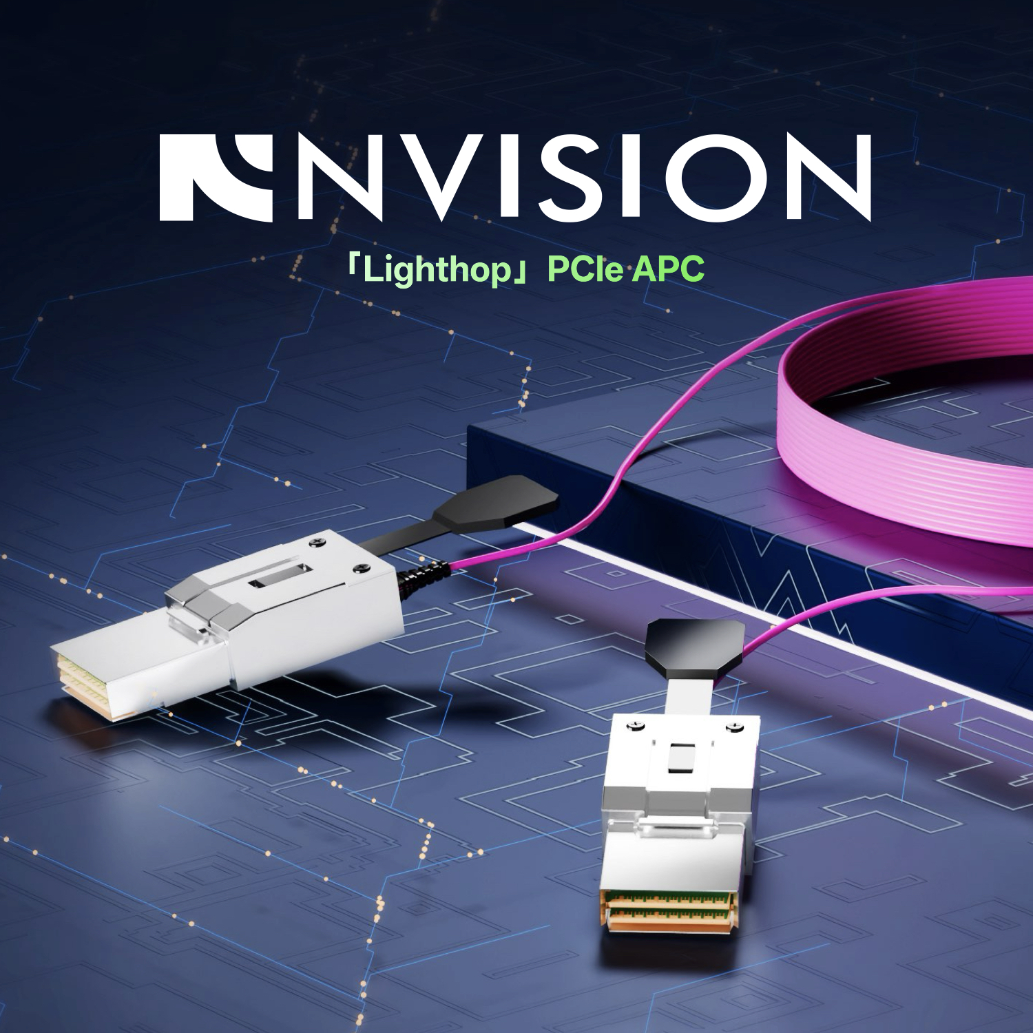 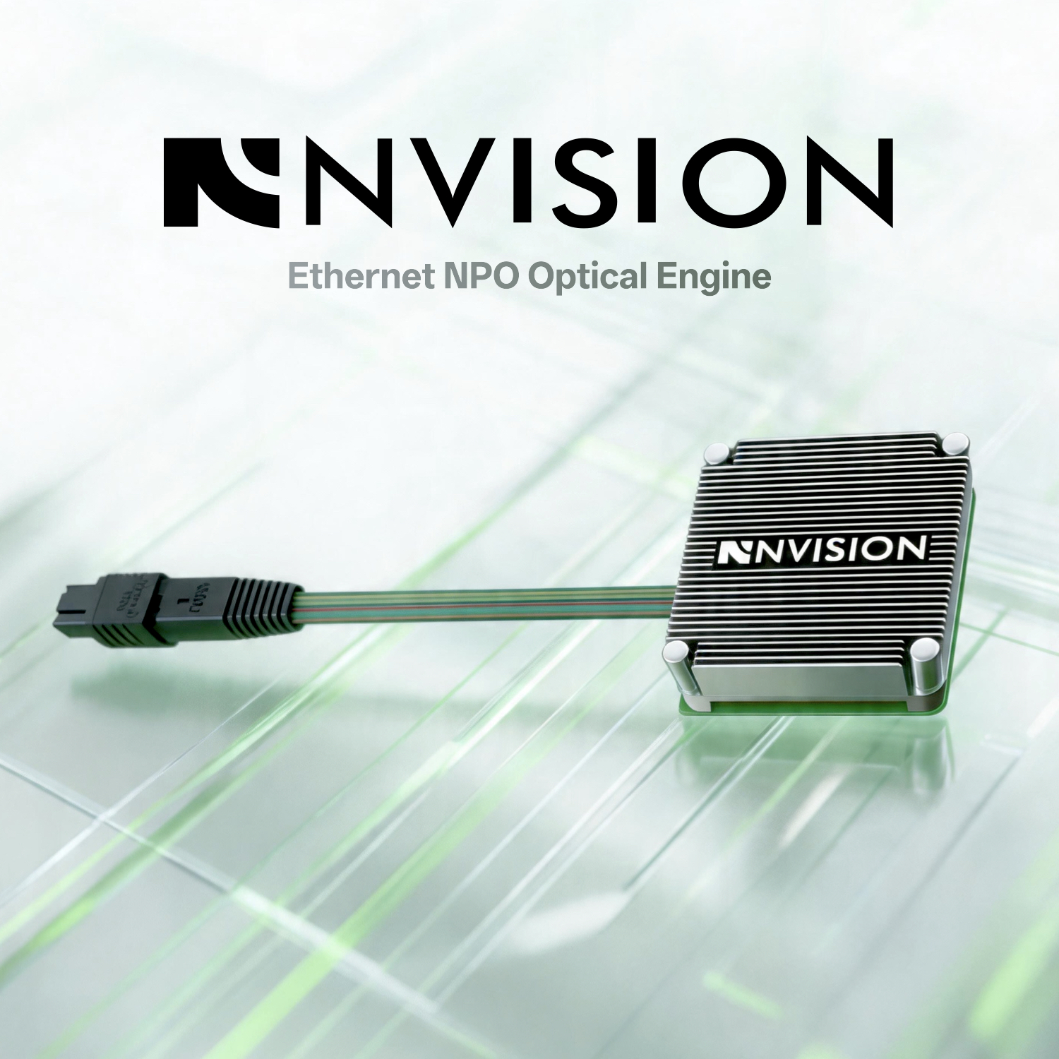 [Video](https://static.glabcms.stoyard.com/stoyard/gallery/20260410/6cmfavklr8w.mp4) [Video](https://static.glabcms.stoyard.com/stoyard/gallery/20260417/yep70h9kzo.m4v) 英伟芯(上海)科技有限公司作为全球研发中心于 2025年3月落户于上海,其充分依托本地完善的半导体生态链(涵盖设计、制造、封测全环节)、顶尖高校及科研机构的高端人才储备,以及政府政策与资本支持,加速硅光芯片的研发与产业化。同时,上海的国际化优势和长三角产业集群协同效应,为技术落地和全球市场拓展提供了强劲支撑。 目前已完成天使轮数千万元融资。  [Video](https://static.glabcms.stoyard.com/stoyard/gallery/20260415/7x6lmtnnpol.mp4) [Video](https://static.glabcms.stoyard.com/stoyard/gallery/20260416/3ai8mntj2nn.mp4)  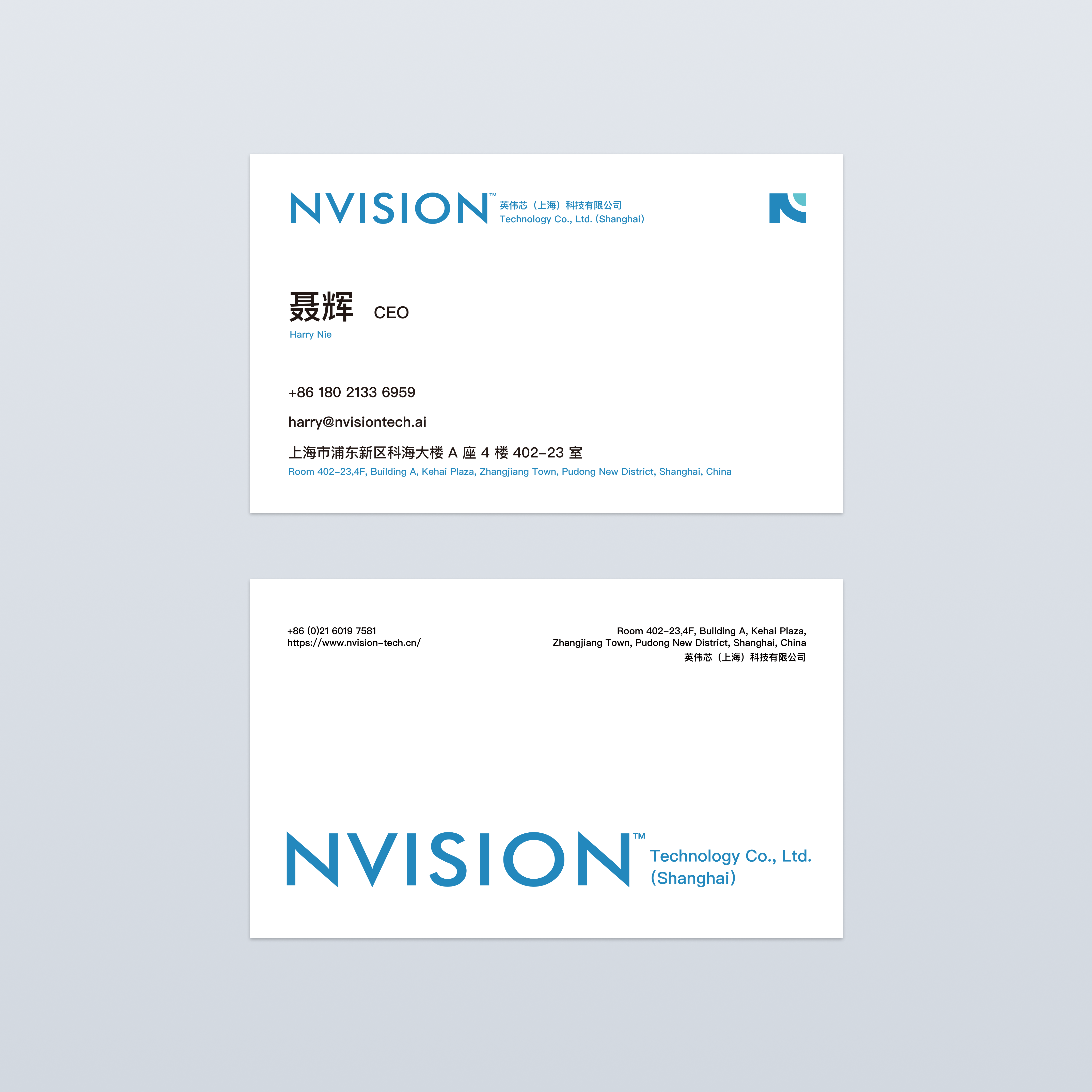 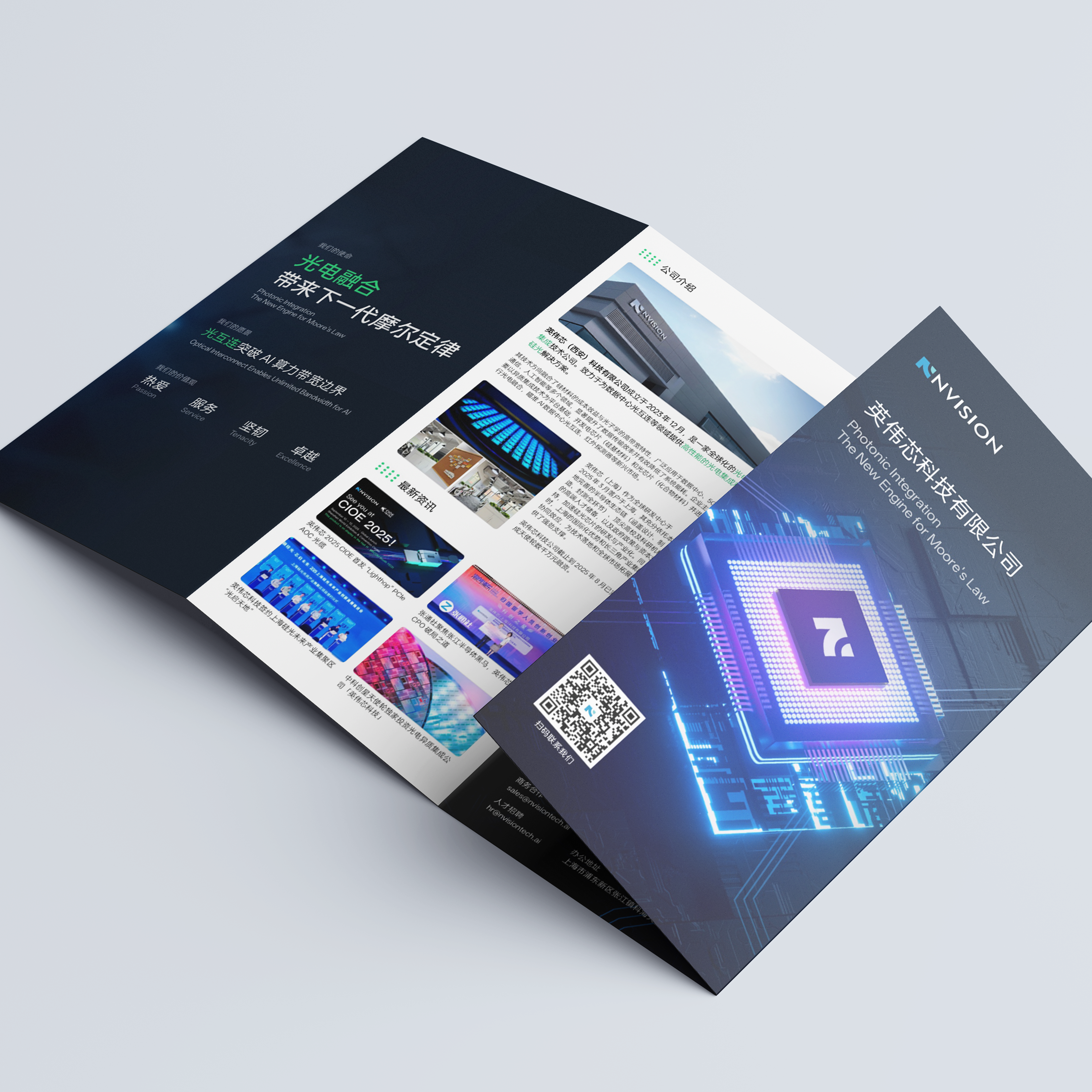  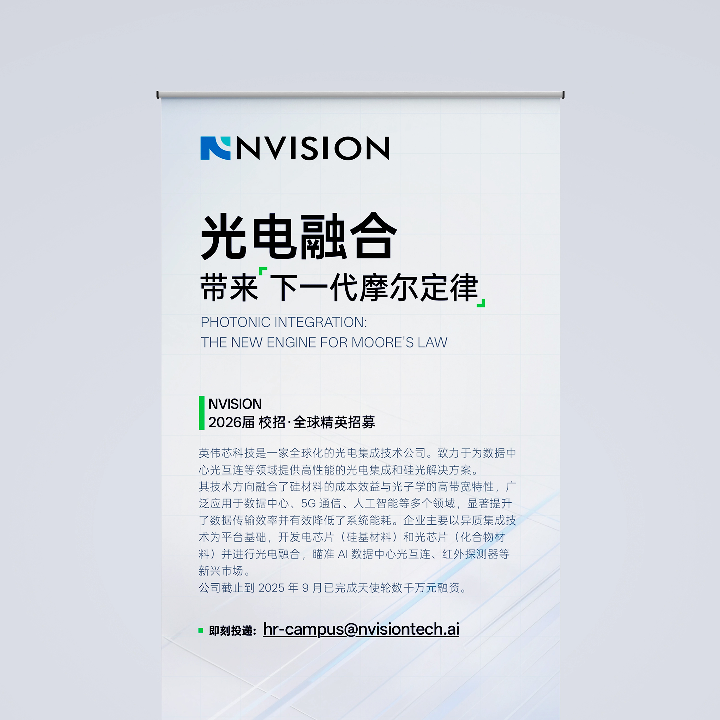  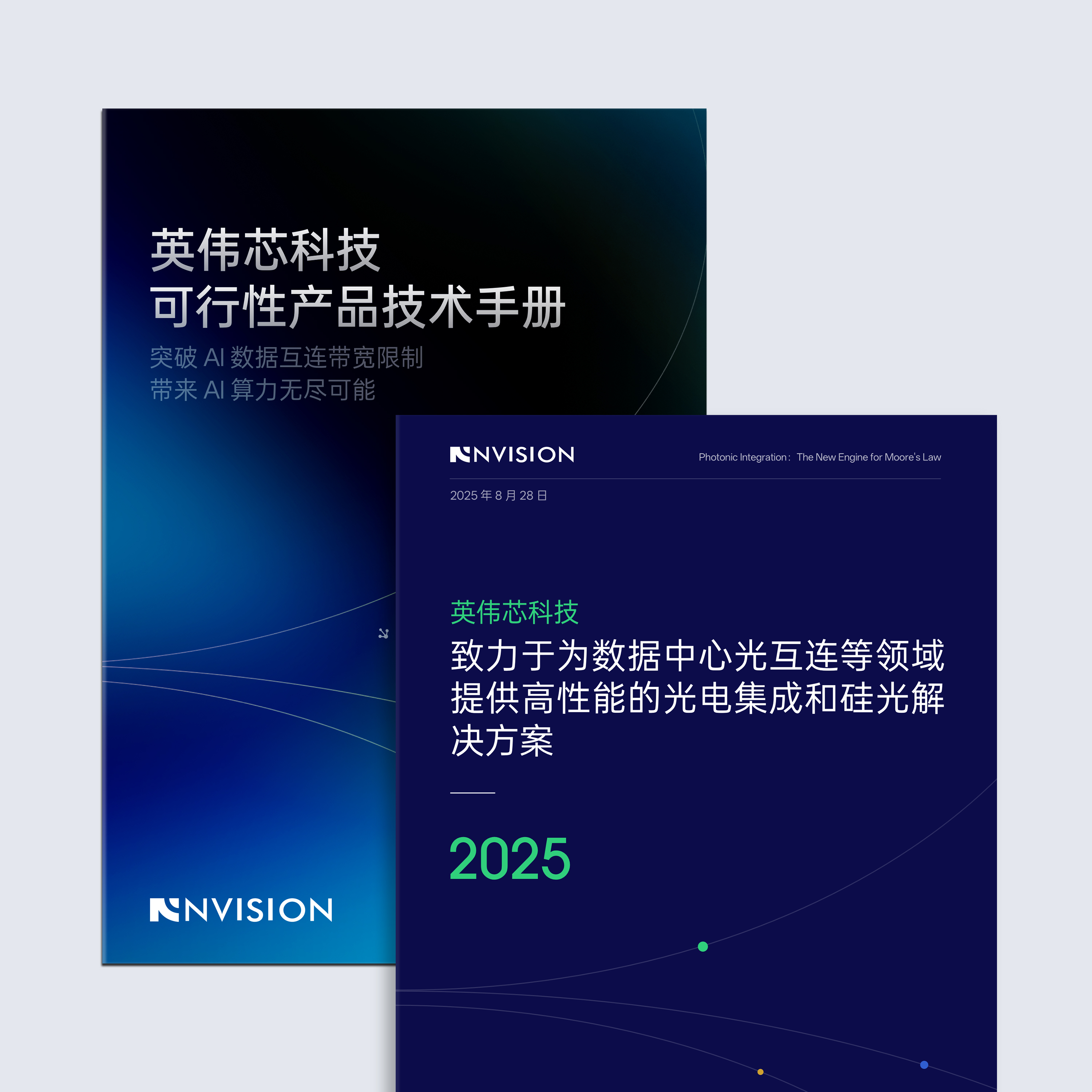 [Video](https://static.glabcms.stoyard.com/stoyard/gallery/20260417/6f1hu09f89b.m4v)  ## English Content ### Introduction Nvision (Xi'an) Technology Co., Ltd., established in December 2023, is a global photonics integration technology company. We strive to deliver high-performance silicon photonics integration with 2.5D and 3D advanced packaging for data center optical interconnect and other applications. Our technology combines "beuties" from both worlds, CMOS cost-effective integrations and high-performance of compound photonic materials. It applicable to data center optical interconnect, AI computing, and other emerging applications such as short-wave infrared detectors. [Video](https://static.glabcms.stoyard.com/stoyard/gallery/20260414/s9qzdq4fk38.mov) This logo to the company's core technology-photoelectric integration for the design of the soul. Through the minimalist geometric language, the high-speed dynamics of "photons" are integrated with the solid foundation of "electronics", which reflects the technical pursuit of high-performance and low-energy data transmission in the field of silicon optical chips. Reconstruction of the letter "N": The icon body is evolved from the brand initials "N" and has a very high degree of recognition. It not only represents NVISION, but also implies New (innovation), Next (future) and Nano (nano-scale precision). The trajectory of photoelectric fusion: the solid block on the left represents a solid silicon-based material and circuit system (electrical chip), symbolizing the enterprise's technological accumulation and industrialization capabilities. Round arc: simulates the propagation path of light waves and the shape of optical fibers, demonstrating the high bandwidth and lightness of photonic technology. Intersection: The perfect embedding of arcs and color blocks accurately and intuitively interprets the core competitiveness of heterogeneous integration-that is, the deep coupling of optical chips and electrical chips. Dynamic sense and speed: The overall upward trend of the icon symbolizes the rapid transmission of data in the data center and AI computing network, and also indicates the rapid rise and vitality of enterprises in the semiconductor circuit. Precise scale: As shown in the auxiliary line diagram, the logo is based on a rigorous golden ratio and a perfect circle cut. The application of this kind of engineering aesthetics reflects the extreme requirement of "micron-level" precision in the semiconductor sealing and testing process, and conveys the craftsman spirit of the enterprise to the product quality.        [Video](https://static.glabcms.stoyard.com/stoyard/gallery/20260410/6cmfavklr8w.mp4) [Video](https://static.glabcms.stoyard.com/stoyard/gallery/20260417/yep70h9kzo.m4v) In March 2025, YingweiXin (Shanghai) Technology Co., Ltd. established its global R&D center in Shanghai. It fully leverages the local complete semiconductor ecosystem (covering the entire process from design, manufacturing to packaging and testing), the reserve of high-end talents from top universities and research institutions, as well as government policies and capital support, to accelerate the research and development and industrialization of silicon photonics chips. Meanwhile, Shanghai's international advantages and the collaborative effect of the Yangtze River Delta industrial clusters provide strong support for technology implementation and global market expansion. We have completed a tens of millions of yuan financing round of angel investment.  [Video](https://static.glabcms.stoyard.com/stoyard/gallery/20260415/7x6lmtnnpol.mp4) [Video](https://static.glabcms.stoyard.com/stoyard/gallery/20260416/3ai8mntj2nn.mp4)        [Video](https://static.glabcms.stoyard.com/stoyard/gallery/20260417/6f1hu09f89b.m4v) 