NVISION
Photonic Integration: The New Engine for Moore's Law
Author: STOYARD 2026-04-01 Editor: STOYARD BEIJING
2025
Nvision (Xi'an) Technology Co., Ltd., established in December 2023, is a global photonics integration technology company. We strive to deliver high-performance silicon photonics integration with 2.5D and 3D advanced packaging for data center optical interconnect and other applications.
Our technology combines "beuties" from both worlds, CMOS cost-effective integrations and high-performance of compound photonic materials. It applicable to data center optical interconnect, AI computing, and other emerging applications such as short-wave infrared detectors.
Our technology combines "beuties" from both worlds, CMOS cost-effective integrations and high-performance of compound photonic materials. It applicable to data center optical interconnect, AI computing, and other emerging applications such as short-wave infrared detectors.
00:00
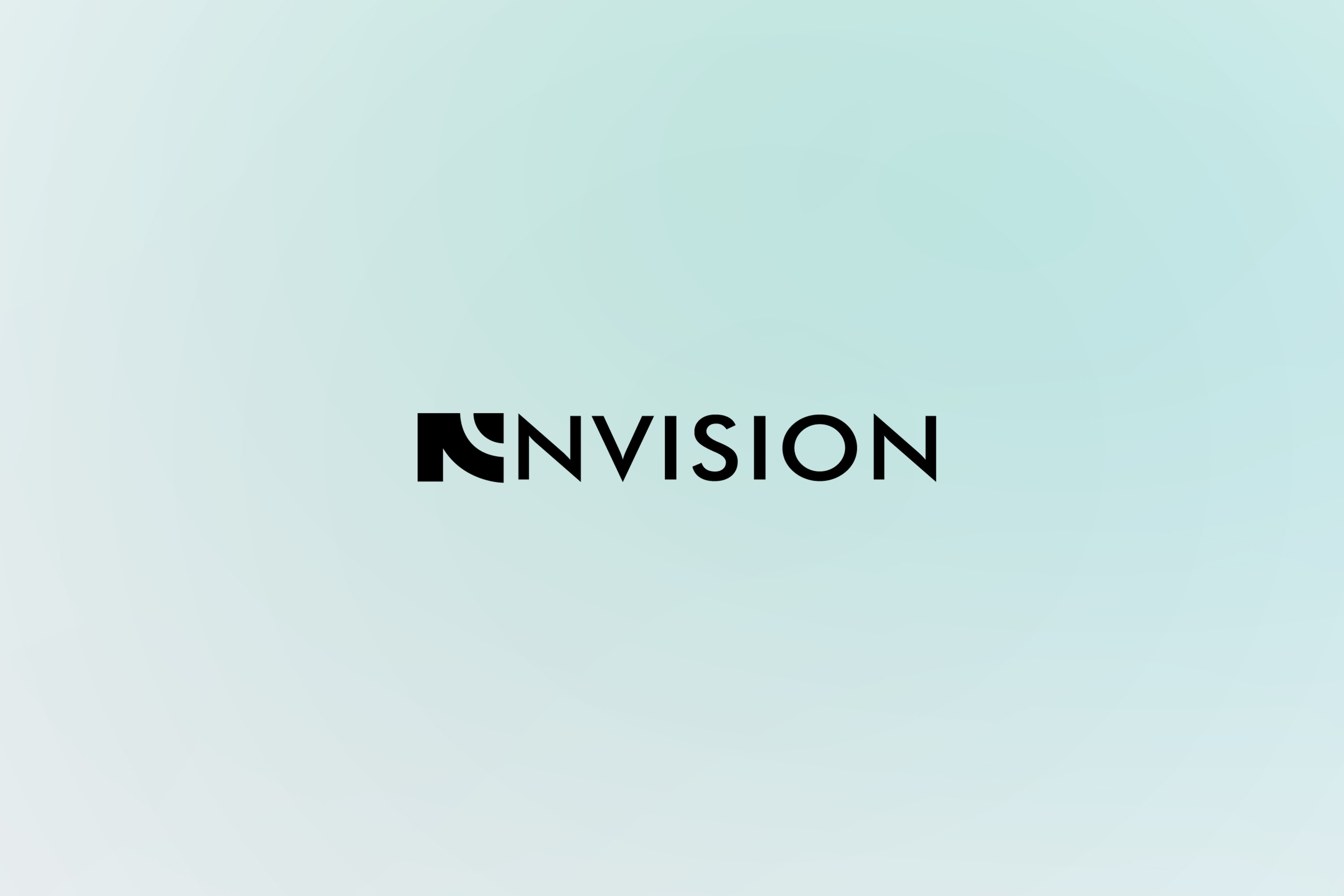
Reconstruction of the letter "N": The icon body is evolved from the brand initials "N" and has a very high degree of recognition. It not only represents NVISION, but also implies New (innovation), Next (future) and Nano (nano-scale precision).
Round arc: simulates the propagation path of light waves and the shape of optical fibers, demonstrating the high bandwidth and lightness of photonic technology.
Intersection: The perfect embedding of arcs and color blocks accurately and intuitively interprets the core competitiveness of heterogeneous integration-that is, the deep coupling of optical chips and electrical chips.
Dynamic sense and speed: The overall upward trend of the icon symbolizes the rapid transmission of data in the data center and AI computing network, and also indicates the rapid rise and vitality of enterprises in the semiconductor circuit.
Precise scale: As shown in the auxiliary line diagram, the logo is based on a rigorous golden ratio and a perfect circle cut. The application of this kind of engineering aesthetics reflects the extreme requirement of "micron-level" precision in the semiconductor sealing and testing process, and conveys the craftsman spirit of the enterprise to the product quality.


1/0

00:00
00:00
We have completed a tens of millions of yuan financing round of angel investment.


00:00
00:00


00:00


Thank for you.
Contact